| CPC H10K 50/115 (2023.02) [H10K 50/16 (2023.02); H10K 71/00 (2023.02); H10K 2102/00 (2023.02); H10K 2102/331 (2023.02)] | 7 Claims |
|
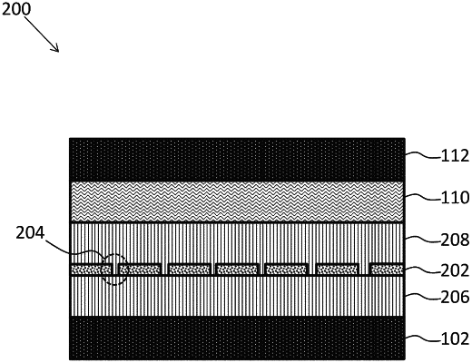
1. A method of forming an illumination device, the method comprising:
disposing a first material over a conductive substrate to form a first material layer, wherein the first material layer is configured as one of a hole transport layer or an electron transport layer;
disposing a layer of luminescent nanostructures over the first material layer, wherein the layer of luminescent nanostructures comprises a plurality of luminescent nanostructures suspended in a polymer layer, wherein the layer of luminescent nanostructures comprises a plurality of discontinuities through a thickness of the layer of luminescent nanostructures, and wherein the plurality of discontinuities is randomly spread over the first material layer;
disposing a second material over the layer of luminescent nanostructures to form a second material layer, wherein the second material is configured as another of the electron transport layer or the hole transport layer, wherein the second material layer directly contacts the first material layer at planar interfaces disposed at the plurality of discontinuities of the layer of luminescent nanostructures, and wherein the planar interfaces are coplanar with a planar bottom surface of the layer of plurality of luminescent nano structures; and
disposing a conductive material over the second material layer.
|