| CPC H10K 10/478 (2023.02) [H01L 27/1214 (2013.01); H10K 59/1213 (2023.02); H10K 59/1216 (2023.02); H10K 59/123 (2023.02); H10K 59/131 (2023.02); H10K 71/00 (2023.02); H10K 50/818 (2023.02); H10K 50/828 (2023.02); H10K 59/122 (2023.02)] | 16 Claims |
|
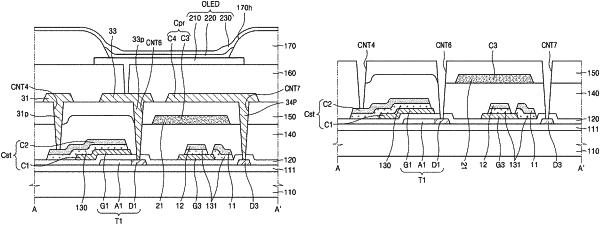
1. A method of providing a display apparatus, the method comprising:
providing a pixel of the display apparatus on a substrate, the providing of the pixel comprising:
providing a first transistor including a gate electrode;
providing a first electrode of a first capacitor;
providing a second electrode of the first capacitor, from a metal material layer, by etching the metal material layer in a first etching process;
providing a first dielectric pattern of the first capacitor, from a dielectric material layer, by etching the dielectric material layer in a second etching process;
providing a third electrode of a second capacitor;
providing an insulating layer including:
a first insulating layer which is between the second electrode of the first capacitor and the third electrode of the second capacitor, and
a second insulating layer which covers the third electrode; and
after the providing of the third electrode of the second capacitor, providing a plurality of contact holes in the insulating layer at which the first transistor and the first capacitor are respectively connected to electrodes outside thereof,
wherein each of the plurality of contact holes is disposed spaced apart from the first dielectric pattern of the first capacitor.
|