| CPC H10B 43/40 (2023.02) [H01L 23/535 (2013.01); H10B 41/27 (2023.02); H10B 41/41 (2023.02); H10B 43/27 (2023.02)] | 18 Claims |
|
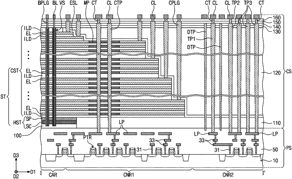
1. A three-dimensional semiconductor memory device, comprising:
a peripheral circuit structure including:
peripheral circuits on a semiconductor substrate,
landing pads connected to the peripheral circuits, and
a lower dielectric layer that covers the peripheral circuits and the landing pads;
an electrode structure on the peripheral circuit structure, the electrode structure including vertically stacked electrodes;
a planarized dielectric layer that covers the electrode structure;
peripheral through plugs spaced apart from the electrode structure, the peripheral through plugs penetrating the planarized dielectric layer to connect to the landing pads;
conductive lines connected through contact plugs, respectively, to the peripheral through plugs; and
at least one dummy through plug adjacent to a first peripheral through plug of the peripheral through plugs, the at least one dummy through plug penetrating the planarized dielectric layer and extending into the lower dielectric layer, and the at least one dummy through plug being in direct contact with the lower dielectric layer and insulated from the conductive lines.
|