| CPC H10B 43/27 (2023.02) [H01L 23/481 (2013.01); H01L 23/528 (2013.01); H10B 43/10 (2023.02); H10B 43/40 (2023.02)] | 20 Claims |
|
1. A semiconductor device comprising:
a substrate including a cell array area and a connecting area, the connecting area including a through-via area;
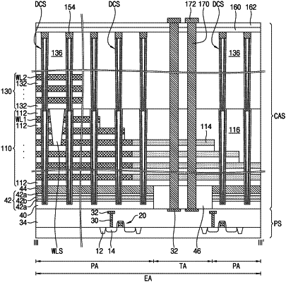
a peripheral circuit structure disposed on the substrate; a lower stack disposed on the peripheral circuit structure and an upper stack disposed on the lower stack, the lower stack including a plurality of lower word lines spaced apart from each other in a vertical direction;
a plurality of channel structures extending through the lower stack and the upper stack in the cell array area;
a plurality of dummy vertical structures extending through the lower stack and the upper stack in the connecting area;
a pair of first separation structures extending vertically through the lower stack and the upper stack and extending in a first horizontal direction, the pair of first separation structures being spaced apart from each other in a second horizontal direction crossing the first horizontal direction; and
a second separation structure disposed at an upper portion of the lower stack and crossing the pair of first separation structures when viewed in a plan view, the second separation structure extending vertically through at least one of the lower word lines and extending in the second horizontal direction.
|