| CPC H10B 43/27 (2023.02) [H10B 41/27 (2023.02); H10B 63/34 (2023.02); H10B 63/845 (2023.02)] | 14 Claims |
|
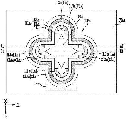
1. A semiconductor device, comprising:
a stacked body including conductive patterns and insulating patterns that are alternately stacked;
a filling layer configured to pass through the stacked body;
a first channel layer configured to pass through the stacked body and coupled to the filling layer;
a second channel layer configured to pass through the stacked body and coupled to the filling layer;
a first interposed layer configured to pass through the stacked body and disposed between the first channel layer and the filling layer;
a second interposed layer configured to pass through the stacked body and disposed between the second channel layer and the filling layer; and
a memory layer configured to surround the filling layer, the first and second channel layers, and the first and second interposed layers, wherein the memory layer includes a first blocking layer, a first data storage layer, and a first tunnel insulating layer adjacent to the first channel layer, and a second blocking layer, a second data storage layer, and a second tunnel insulating layer adjacent to the second channel layer,
the first blocking layer and the second blocking layer are coupled to each other, the first data storage layer and the second data storage layer are coupled to each other, and the first tunnel insulating layer and the second tunnel insulating layer are coupled to each other, and
an entirety of an inside wall of the first channel layer is in contact with the first interposed layer and an entirety of an inside wall of the second channel layer is in contact with the second interposed layer.
|