| CPC H10B 43/27 (2023.02) [H01L 29/66833 (2013.01); H01L 29/7926 (2013.01); H10B 43/35 (2023.02)] | 20 Claims |
|
1. A non-volatile storage device, comprising:
a first layer;
a second layer over the first layer;
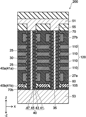
a stacked body including a plurality of conductive films stacked above the second layer; and
a semiconductor pillar which penetrates the stacked body and the second layer and reaches the first layer, wherein
the semiconductor pillar includes a semiconductor film provided along an extending direction of the semiconductor pillar and a memory film provided on a periphery of the semiconductor film,
the memory film includes a first portion between the stacked body and the semiconductor film in a direction perpendicular to the extending direction and a second portion between the second layer and the semiconductor film in the direction perpendicular to the extending direction, and
a thickness of the second portion of the memory film in the semiconductor pillar is greater than a thickness of the first portion of the memory film in the semiconductor pillar.
|