| CPC H10B 43/27 (2023.02) [H10B 41/10 (2023.02); H10B 41/27 (2023.02); H10B 41/35 (2023.02); H10B 43/10 (2023.02); H10B 43/35 (2023.02)] | 19 Claims |
|
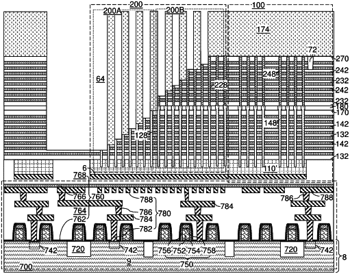
1. A method of forming a three-dimensional memory device, comprising:
forming a first-tier alternating stack of first insulating layers and first sacrificial material layers over a substrate;
forming a joint dielectric layer over the first-tier alternating stack, wherein the joint dielectric layer is thicker than each of the first insulating layers and the first sacrificial material layers;
forming first-tier memory openings and first-tier support openings through the first-tier alternating stack and the joint dielectric layer;
forming sacrificial first-tier memory opening fill portions in the first-tier memory openings in a memory array region and forming sacrificial first-tier support opening fill portions in the first-tier support openings in an area outside of the memory array region;
forming a second-tier alternating stack of second insulating layers and second sacrificial material layers over the joint dielectric layer, the first-tier alternating stack and the sacrificial first-tier memory opening fill portions;
performing a level-shift anisotropic etch process to form a recess trench vertically extending through the second-tier alternating stack and down to the joint dielectric layer in a staircase region, wherein top surfaces of a first subset of the sacrificial first-tier support opening fill portions are exposed underneath the recess trench and a second subset of the sacrificial first-tier support opening fill portions located outside an area of a volume of the recess trench are not exposed to the recess trench, wherein an entirety of the recess trench has a uniform depth throughout and each sidewall of the recess trench is a vertical sidewall which extends straight from a top surface of the joint dielectric layer at least to a respective edge of a topmost surface of the second-tier alternating stack;
performing an extension etching process to extend the recess trench through at least the joint dielectric layer by removing portions of the joint dielectric layer that underlie the recess trench in the staircase region, wherein at least one of etching time or etching power used during the extension etching process is different from that used during the level-shift anisotropic etch process;
patterning first stepped surfaces in the first-tier alternating stack underneath the volume of the recess trench and patterning second stepped surfaces in the second-tier alternating stack adjacent to, and outside the area of, the volume of the recess trench, whereby a continuous stepped cavity overlying the first stepped surfaces and the second stepped surfaces is formed in the staircase region, whereby upper portions of the first subset of the sacrificial first-tier support opening fill portions are removed during patterning of the first stepped surfaces;
removing lower portions of the first subset of the sacrificial first-tier support opening fill portions after formation of the first stepped surfaces, whereby vertically-extending voids formed by removal of the lower portions of the first subset of the sacrificial first-tier support opening fill portions vertically extend through the first-tier alternating stack;
forming a retro-stepped dielectric material portion in a combination of the continuous stepped cavity and the vertically-extending voids, wherein the retro-stepped dielectric material portion comprises vertically-extending portions that vertically extend through a respective subset of layers within the first-tier alternating stack and fill volumes of the vertically-extending voids;
forming memory openings through the second-tier alternating stack and the first-tier alternating stack, wherein each of the memory openings comprises a volume formed by removing a respective one of the sacrificial first-tier memory opening fill portions;
forming memory opening fill structures in the memory openings, wherein each of the memory opening fill structures comprises a respective vertical semiconductor channel and a respective vertical stack of memory elements; and
replacing the first sacrificial material layers and the second sacrificial material layers with first electrically conductive layers and second electrically conductive layers, respectively.
|