| CPC H10B 43/27 (2023.02) [H01L 23/5226 (2013.01); H10B 43/10 (2023.02)] | 19 Claims |
|
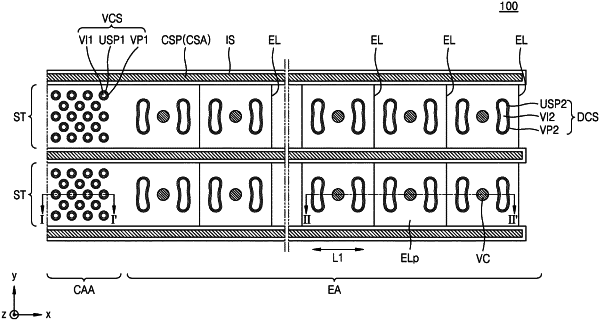
1. A vertical type non-volatile memory device comprising:
a substrate having a cell array area and an extension area extending in a first direction from the cell array area, the first direction extending parallel to a top surface of the substrate;
a vertical contact disposed on the substrate in the extension area and extending in a vertical direction perpendicular to the top surface of the substrate;
a plurality of vertical channel structures on the substrate in the cell array area and extending in the vertical direction;
a plurality of dummy channel structures on the substrate in the extension area and extending in the vertical direction and disposed adjacent to the vertical contact;
a plurality of gate electrode layers and a plurality of interlayer insulation layers stacked alternately on the substrate in the cell array area and the extension area along sidewalls of the plurality of vertical channel structures and the plurality of dummy channel structures; and
an electrode pad connected to the vertical contact, wherein:
in the electrode pad, first and second dummy channel structures, from among the plurality of dummy channel structures, are respectively disposed at a first side of the vertical contact in the first direction, and third and fourth dummy channel structures, from among the plurality of dummy channel structures, are respectively disposed at a second side of the vertical contact opposite the first side in the first direction,
a horizontal cross-sectional surface of each of the first through fourth dummy channel structures has a shape that is longer in a second direction than in the first direction, the second direction extending parallel to the top surface of the substrate and perpendicular to the first direction,
shapes of the first and second dummy channel structures are symmetrical with respective shapes of the third and fourth dummy channel structures relative to the vertical contact centered therebetween, and
the plurality of dummy channel structures extend lengthwise in the second direction and have a bent structure rather than a straight line.
|
|
12. A vertical type non-volatile memory device comprising:
a substrate having a cell array area and an extension area extending in a first direction from the cell array area, the first direction extending parallel to a top surface of the substrate;
a vertical contact disposed on the substrate in the extension area and extending in a vertical direction perpendicular to the top surface of the substrate;
a plurality of dummy channel structures on the substrate in the extension area and extending in the vertical direction and disposed adjacent to the vertical contact;
a plurality of gate electrode layers and a plurality of interlayer insulation layers stacked alternately on the substrate in the cell array area and the extension area along sidewalls of the plurality of dummy channel structures;
an electrode pad connected to the vertical contact, wherein:
the electrode pad comprises:
first and second dummy channel structures from among the plurality of dummy channel structures disposed at a first side of the vertical contact in the first direction and third and fourth dummy channel structures from among the plurality of dummy channel structures disposed at a second side of the vertical contact opposite the first side in the first direction; and
a division area extending in the first direction and dividing the plurality of gate electrode layers in a second direction, the second direction extending parallel to the top surface of the substrate and perpendicular to the first direction,
shapes of the first and second dummy channel structures are symmetrical with respective shapes of third and fourth dummy channel structures relative to the vertical contact centered therebetween, and
the plurality of dummy channel structures extend in the second direction and have a bent structure rather than a straight line.
|