| CPC H10B 41/27 (2023.02) [G11C 5/025 (2013.01); G11C 5/06 (2013.01); H01L 21/3065 (2013.01); H01L 21/31053 (2013.01); H01L 21/67075 (2013.01); H01L 21/76876 (2013.01); H01L 29/04 (2013.01); H10B 43/27 (2023.02)] | 20 Claims |
|
1. A semiconductor memory device comprising:
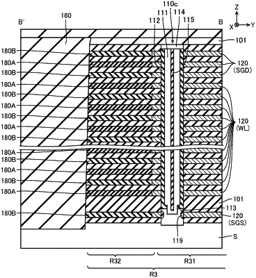
a substrate including a first region over which a plurality of memory cells for storing data are disposed and a second region arranged on an outer side of the first region in a first direction;
a stacked structure including a plurality of conductive layers separated from each other in the stacked structure in a second direction perpendicular to the first direction above the first region of the substrate and including a plurality of first layers separated from each other in the stacked structure in the second direction above the second region of the substrate; and
a plurality of columnar structures that extend in the second direction and are opposed to the conductive layers above the first region of the substrate, the columnar structures forming the memory cells at intersections with at least some of the plurality of conductive layers, wherein
the conductive layers include a plurality of first conductive layers and a plurality of second conductive layers arranged in the second direction, and the first layers include a plurality of first films disposed in same layers as the first conductive layers and a plurality of second films disposed in same layers as the second conductive layers, the first and second films being arranged in the second direction, the first films being different in material from the first conductive layers, the second films being different in material from the second conductive layers,
the first conductive layers of the conductive layers and the first films of the first layers in the stacked structure are coupled with each other in the first direction, and the second conductive layers of the conductive layers and the second films of the first layers in the stacked structure are coupled with each other in the first direction, and
respective coupling portions of the first films with the first conductive layers are farther from the first region in the first direction than respective coupling portions of the second films with the second conductive layers.
|