| CPC H10B 12/50 (2023.02) [H10B 12/33 (2023.02); G11C 5/063 (2013.01)] | 20 Claims |
|
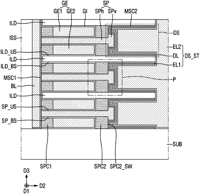
1. A semiconductor memory device comprising:
at least one bit line on a semiconductor substrate, the at least one bit line extending in a first direction perpendicular to a top surface of the semiconductor substrate;
at least one semiconductor pattern including a horizontal portion extending in a second direction parallel to the top surface of the semiconductor substrate and a vertical portion extending in the first direction, a first end of the horizontal portion of the at least one semiconductor pattern being connected to the at least one bit line, and a second end of the horizontal portion of the at least one semiconductor pattern being connected to the vertical portion of the at least one semiconductor pattern;
at least one gate electrode on the horizontal portion of the at least one semiconductor pattern and extending in a third direction different from the first direction and the second direction; and
at least one information storage element connected to the vertical portion of the at least one semiconductor pattern,
wherein a thickness of the horizontal portion of the at least one semiconductor pattern in the first direction is smaller than a thickness of the vertical portion of the at least one semiconductor pattern in the first direction, and
wherein the at least one gate electrode does not overlap the vertical portion of the semiconductor pattern in the first direction.
|