| CPC H10B 12/30 (2023.02) [G11C 5/063 (2013.01); H10B 12/03 (2023.02); H10B 12/482 (2023.02); H10B 12/485 (2023.02); H10B 12/488 (2023.02); H01L 27/0688 (2013.01)] | 29 Claims |
|
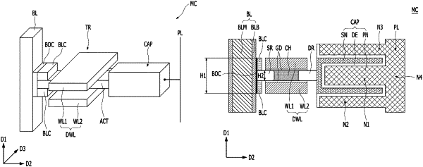
8. A semiconductor memory device, comprising:
a transistor laterally extending in a direction parallel to a substrate and including an active layer over the substrate, the active layer having a first end and a second end;
bit line contact nodes formed on an upper surface and a lower surface of the first end of the active layer, respectively;
a bit line side-ohmic contact vertically extending and connecting to the first end of the active layer and the bit line contact nodes;
a bit line extending in a vertical direction to the substrate and connected to the bit line side-ohmic contact;
storage contact nodes formed on an upper surface and a lower surface of the second end of the active layer, respectively;
a storage node side-ohmic contact vertically extending and connecting to the second end of the active layer and the storage contact nodes; and
a capacitor connected to the storage node side-ohmic contact,
wherein the bit line side-ohmic contact and the storage node side-ohmic contact include a metal silicide, and
wherein each of the bit line contact nodes and the storage contact nodes includes doped polysilicon.
|