| CPC H10B 12/30 (2023.02) [H10B 12/03 (2023.02); H10B 12/05 (2023.02)] | 19 Claims |
|
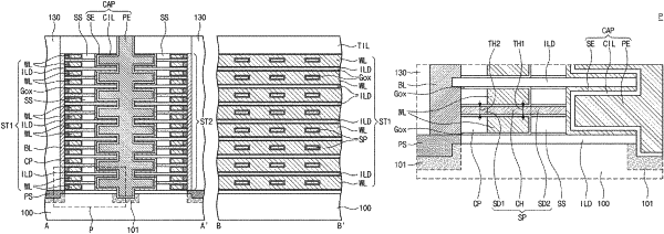
1. A semiconductor memory device, comprising:
a substrate;
a stack including a plurality of word lines and a plurality of interlayer insulating patterns, which are alternatingly stacked on the substrate,
wherein the word lines extend in a first direction substantially parallel to a top surface of the substrate;
a plurality of semiconductor patterns crossing the word lines and having longitudinal axes that are substantially parallel to a second direction,
wherein the semiconductor patterns are spaced apart from each other in the first direction and a third direction that is substantially perpendicular to the top surface of the substrate;
a plurality of bit lines extending in the third direction and spaced apart from each other in the first direction,
wherein each of the bit lines is in contact with first side surfaces of the semiconductor patterns that are spaced apart from each other in the third direction;
a plurality of data storage elements,
wherein the data storage elements are respectively provided between vertically adjacent patterns of the interlayer insulating patterns and are in contact with second side surfaces opposite to the first side surfaces of the semiconductor patterns; and
a plurality of substrate impurity layers provided in portions of the substrate at both sides of the stack.
|