| CPC H04N 25/76 (2023.01) [G01S 7/4863 (2013.01); G01S 17/894 (2020.01); H01L 27/14607 (2013.01)] | 20 Claims |
|
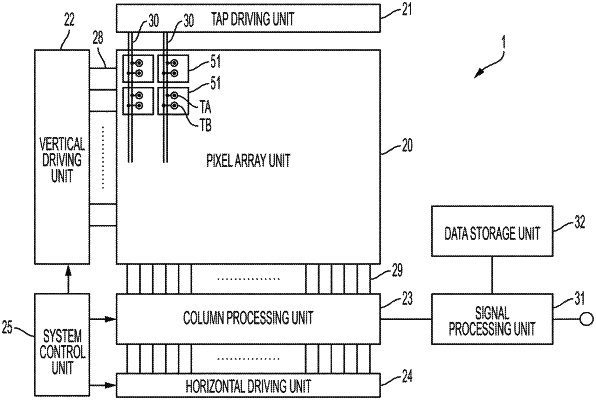
1. An imaging device, comprising:
a pixel array including a plurality of pixels, each pixel including:
a photoelectric conversion region that converts incident light into electric charge; and
a charge transfer section coupled to the photoelectric conversion region and having line symmetry along a first axis that passes through the charge transfer section in a plan view, the charge transfer section including:
a first transfer transistor coupled to a first floating diffusion and the photoelectric conversion region and located within a first half of the pixel in the plan view;
a second transfer transistor coupled to a second floating diffusion and the photoelectric conversion region and located within the first half of the pixel in the plan view; and
a third transfer transistor coupled to the photoelectric conversion region and an overflow region and located within the first half of the pixel between the first transfer transistor and the second transfer transistor in the plan view.
|