| CPC H04N 23/61 (2023.01) [G06N 3/04 (2013.01)] | 7 Claims |
|
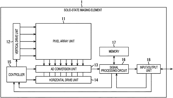
1. A solid-state imaging element, comprising:
a calculation unit configured to:
execute a calculation, of at least one stage of a convolutional layer and a pooling layer in a convolutional neural network, on a signal corresponding to a light reception amount of light incident on each pixel of a pixel array unit;
change, based on a coefficient corresponding to the calculation of the convolutional layer, a capacity ratio of a capacitive element configured to hold the signal different for each pixel of the pixel array unit; and
multiply the signal by the coefficient corresponding to the calculation of the convolutional layer based on the changed capacity ratio of the capacitive element.
|