| CPC H04N 23/54 (2023.01) [H04N 23/55 (2023.01); H04N 23/57 (2023.01)] | 20 Claims |
|
1. A photosensitive assembly, characterized by comprising:
a photosensitive chip, including a photosensitive area and an electric connection area located around the photosensitive area;
at least one resistance-capacitance device;
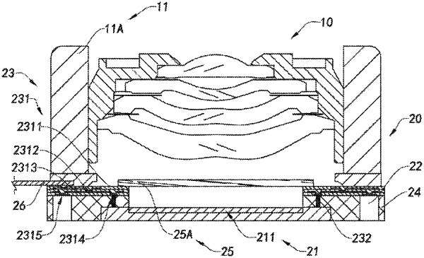
an expanded wiring assembly, wherein the photosensitive chip and the at least one resistance-capacitance device is electrically connected to the expanded wiring assembly, respectively, so that the at least one resistance-capacitance device and the photosensitive chip are conducted by means of the expanded wiring assembly, and the expanded wiring assembly includes an expanded wiring layer having a top surface and a bottom surface and a conducting element, and the at least one resistance-capacitance device is electrically connected to the bottom surface of the expanded wiring layer, and the conducting element extends between the bottom surface of the expanded wiring layer and the electric connection area of the photosensitive chip, so as to electrically connect the photosensitive chip to the expanded wiring layer by means of the conducting element, and a light hole is formed in the expanded wiring layer and corresponds to at least the photosensitive area of the photosensitive chip; and
a molded base, in which the photosensitive chip and the resistance-capacitance device are received respectively and on which the expanded wiring layer is supported;
wherein the expanded wiring layer includes an expanded circuit having a first electric connection end and a second electric connection end, and the first electric connection end is electrically connected to the conducting element, and the second electric connection end extends laterally from the first electric connection end in a direction away from the conducting element and is electrically connected to the at least one resistance-capacitance device.
|