| CPC H04L 27/0014 (2013.01) [H04L 27/06 (2013.01); H04L 27/12 (2013.01); H04L 2027/0026 (2013.01)] | 1 Claim |
|
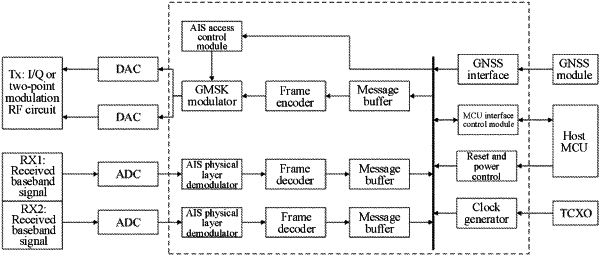
1. A system for processing an automatic identification system (AIS) baseband signal based on a field-programmable gate array (FPGA), comprising an FPGA functional block and a peripheral circuit, wherein the peripheral circuit comprises a digital to analog converter (DAC), an analog to digital converter (ADC), a host microprogrammed control unit (MCU), a global navigation satellite system (GNSS) module, a temperature compensated crystal oscillator (TCXO), and a reset and power control module; the FPGA functional block comprises a bus, a plurality of message buffers, an AIS access control module, a Gaussian filtered minimum shift keying (GMSK) modulator, a frame encoder, an AIS physical layer demodulator, and a frame decoder; an output of the bus is connected to one message buffer and one AIS access control module; an output of the AIS access control module is connected to the GMSK modulator; the one message buffer connected to the output of the bus is connected to the frame encoder; an output of the frame encoder is connected to the GMSK modulator; and a signal output by the bus is cached in the one message buffer and then sent to the GMSK modulator after being encoded by the frame encoder; another signal output by the bus is processed by the AIS access control module and then also sent to the GMSK modulator; the two signals output by the bus are respectively output to two DACs after being modulated by the GMSK modulator; an analog signal is converted into a digital signal, and the digital signal is sent to an in-phase and quadrature (I/Q) or two-point modulation radio frequency (RF) circuit; and two received baseband signals are respectively input into ADCs and separately sent to the bus through the AIS physical layer demodulator, the frame decoder, and a second message buffer of the plurality of message buffers in sequence;
the TCXO enables a clock generator to generate a stable-frequency clock pulse, and is connected to the bus to output the stable-frequency clock pulse to the bus; the host MCU is connected to an MCU interface control module and then connected to the bus, and the host MCU is also connected to the reset and power control module to provide power input and reset functions; and the GNSS module is connected to a GNSS interface of the FPGA functional block, such that the GNSS module is connected;
the AIS access control module is responsible for accessing an AIS signal, comprising AIS timeslot calculation and sending time window control; the one message buffer is connected to the frame encoder, and the output of the frame encoder is connected to the GMSK modulator;
and the frame encoder is responsible for packaging a physical frame of the AIS signal, comprising filling a bit, adding a training sequence, and operating a frame start signal, a cyclic redundancy check (CRC) signal, and a frame end signal;
the GMSK modulator is configured to modulate the AIS signal, wherein in order to reduce use of an FPGA logic unit, a modulation of the GMSK modulator is specifically implemented as follows by using a look-up table (LUT): inputting data, generating a phase path table, obtaining a phase at a current time point, calculating I and Q signals, generating a corresponding LUT, and obtaining I and Q signals at the current time point based on the LUT;
the AIS physical layer demodulator is a demodulator for the AIS baseband signal, and internally comprises synchronization and demodulation processes and outputs a bit output sequence obtained after AIS demodulation; and
a count calibration of the AIS access control module is as follows: the AIS access control module first calculates an accurate start point of an AIS timeslot based on a serial port signal and a pulse-per-second signal that are connected to the GNSS module; and the GNSS module generates a pulse signal per second, with an accuracy of up to nanoseconds, waits for the generated pulse signal per second, inputs read serial port time, and adjusts and calibrates an internal timer in the case of even seconds, or waits again for the generated pulse signal per second in the case of non-even seconds.
|