| CPC H04L 25/03057 (2013.01) [H04L 25/03006 (2013.01)] | 10 Claims |
|
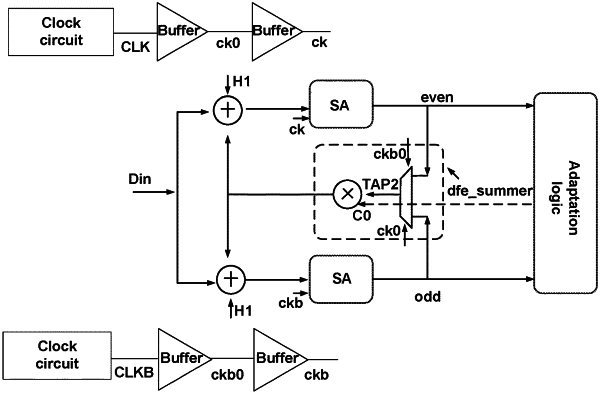
1. A decision feedback equalizer circuit, comprising:
a first adder circuit configured to receive sampled data, first correction data and target correction data output by a correction parameter processing element and add the sampled data, the first correction data and the target correction data to obtain a first calculation result;
a first sampler amplifier connected with the first adder circuit and configured to sample the first calculation result output by the first adder circuit according to a first signal component in a first clock signal to obtain a first sampling result of a present sampling period;
a second adder circuit configured to receive the sampled data, the first correction data and the target correction data output by the correction parameter processing element and add the sampled data, the first correction data and the target correction data to obtain a second calculation result;
a second sampler amplifier, connected with the second adder circuit and configured to sample the second calculation result output by the second adder circuit according to a second signal component in the first clock signal to obtain a second sampling result of the present sampling period, signal change directions of the second signal component and the first signal component being opposite; and
the correction parameter processing element connected with the first sampler amplifier and the second sampler amplifier, respectively, and configured to determine the first sampling result or the second sampling result as a target correction value according to a second clock signal and determine the target correction data based on the target correction value, a time sequence of the second clock signal being prior to a time sequence of the first clock signal, such that components of the target correction data in the first sampling result obtained by sampling of the first sampler amplifier and the second sampling result obtained by sampling of the second sampler amplifier meet a preset requirement.
|