| CPC H03M 13/6356 (2013.01) [G06F 11/1076 (2013.01); G06F 13/1678 (2013.01)] | 19 Claims |
|
1. An integrated circuit, comprising:
data utilization circuitry configurable to generate first data characterized by a first data width; and
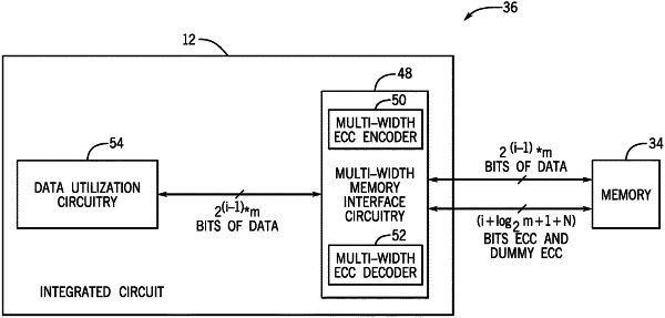
configurable error correction code (ECC) circuitry communicatively coupled between the data utilization circuitry and a memory comprising a memory interface, wherein the configurable ECC circuitry comprises an encoder having a second data width, and wherein the configurable ECC circuitry is configurable to:
receive the first data from the data utilization circuitry;
adjust the first data characterized by the first data width into second data characterized by the second data width configurable to be processed by the encoder to generate ECC bits before being stored in the memory, wherein the encoder is configurable to generate the ECC bits based on a logarithmic relationship between the first data width and the second data width;
process, via an output format converter, the ECC bits to pad the ECC bits with one or more dummy ECC bits to match a width of the ECC bits padded by the one or more dummy ECC bits to a width of the memory interface; and
write the ECC bits padded by the one or more dummy ECC bits to the memory.
|