| CPC H03M 1/1255 (2013.01) [G11C 7/1036 (2013.01); H03K 19/1774 (2013.01); H03M 1/1215 (2013.01)] | 18 Claims |
|
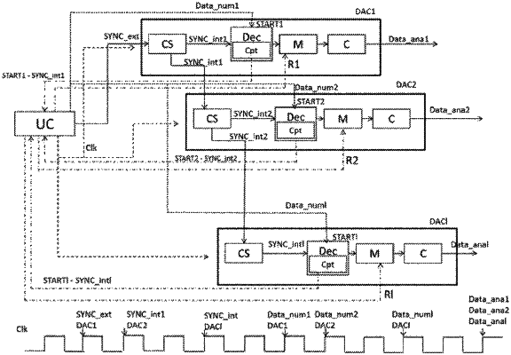
1. A method for synchronizing analog data (Data_ana1, Data_ana2, Data_ana1) at an output of a plurality of digital/analog converters (DAC, DAC1, DAC2, DACI), comprising at least one conversion core (C, C1, C2), on an active edge of a common reference clock (Clk), characterized in that the method comprises the following steps:
a) Supplying an external synchronization signal (SYNC_ext), emitted by a control unit (UC), to at least one converter of the plurality of converters, and supplying a clock signal of the common reference clock to the plurality of converters;
b) Generating, within each converter of the plurality of converters, an internal synchronization signal (SYNC_int, SYNC_int1, SYNC_int2, SYNC_int1) from the external synchronization signal, such that all the internal synchronization signals are aligned on an active edge of the common reference clock;
c) Generating, by means of at least one electronic circuit internal to each converter of the plurality of converters, a start signal (START1, START2, STARTI) which represents a start of sending of digital data (Data_num1, Data_num2, Data_num1) by the control unit, on each core of the plurality of converters, and counting a number of clock strokes between the generation of the start signal and the generation of the internal synchronization signal for each of the cores of the plurality of converters; and
d) Applying a delay Ri (R1, R2, RI) to each core i of the plurality of converters, the delay being equal to the difference between the highest number counted in step c) and the number counted in step c) for the core i, i being an integer between 1 and the number of cores of the plurality of converters.
|