| CPC H03M 1/1245 (2013.01) [H03K 17/54 (2013.01)] | 16 Claims |
|
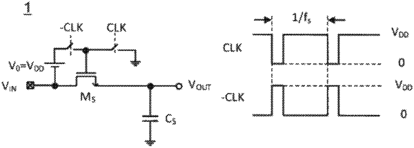
1. A sampling switch circuit, comprising:
an input node, connected to receive an input voltage signal;
a sampling transistor comprising a gate terminal, a source terminal and a drain terminal, the source terminal connected to the input node;
a hold-control node connected to receive a hold-control voltage signal;
an output node connected to the drain terminal of the sampling transistor;
a buffer circuit having a buffer input connected to the input node and a buffer output connected to a track-control node, the buffer circuit configured to provide a track-control voltage signal at the track-control node dependent on the input voltage signal; and
switching circuitry configured to connect the gate terminal of the sampling transistor to the track-control node or to the hold-control node in dependence upon a clock signal.
|