| CPC H03M 1/004 (2013.01) [H03M 1/0626 (2013.01); H03M 1/0854 (2013.01); H03M 1/1245 (2013.01); H03M 1/34 (2013.01); H03M 3/462 (2013.01); H03M 3/476 (2013.01); H03M 3/422 (2013.01)] | 20 Claims |
|
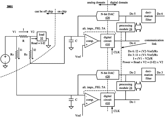
1. A power sensing circuit comprising:
a first analog to digital converter (ADC) operably coupled to a first terminal of a first in-line resistor via a first single line and configured to process a first digital output signal to generate a second digital output signal that is representative of a first difference between a first in-line resistor voltage of the first terminal of the first in-line resistor and a first reference voltage;
a second ADC operably coupled to a first terminal of a second in-line resistor via a second single line and configured to process a third digital output signal to generate a fourth digital output signal that is representative of a second difference between a second in-line resistor voltage of the first terminal of the second in-line resistor and a second reference voltage, and wherein:
both the first in-line resistor and the second in-line resistor have a common resistance value;
memory that stores operational instructions; and
one or more processing modules, wherein, when enabled, configured to execute the operational instructions to:
determine a first measurement resistor voltage of a first terminal of a measurement resistor and a second measurement resistor voltage of a second terminal of the measurement resistor based on the second digital output signal associated with the first ADC and the fourth digital output signal associated with the second ADC, wherein the measurement resistor operably coupled between a second terminal of the first in-line resistor and a second terminal of the second in-line resistor;
determine a measurement resistor current through the measurement resistor based on the first measurement resistor voltage, the second measurement resistor voltage, and the measurement resistor; and
determine a power delivered to a load that is operably coupled to the second terminal of the measurement resistor based on the measurement resistor current, a second in-line resistor current associated with the second in-line resistor of the second ADC, and the second measurement resistor voltage of the second terminal of the measurement resistor.
|