| CPC H03K 3/012 (2013.01) | 14 Claims |
|
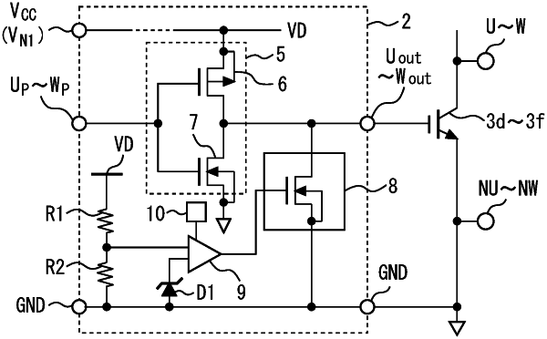
1. A semiconductor device comprising:
a first terminal inputting a first voltage from outside the semiconductor device;
a drive unit using the first voltage as a power supply voltage and outputting a drive signal;
a switching device driven by the drive signal;
a second terminal separated from the first terminal and inputting a second voltage, the second voltage being input even when the first voltage is turned off;
a comparator using a voltage generated from the second voltage as a power supply voltage and outputting an output signal when a voltage generated from the first voltage is less than or equal to a reference potential, the voltage generated from the first voltage being applied to an input terminal of the comparator; and
a shut-off switch shutting off a transmission of the drive signal to the switching device from the drive unit in response to the output signal.
|