| CPC H03K 3/011 (2013.01) [H03K 3/012 (2013.01); H03K 17/6872 (2013.01); H03K 17/6874 (2013.01)] | 20 Claims |
|
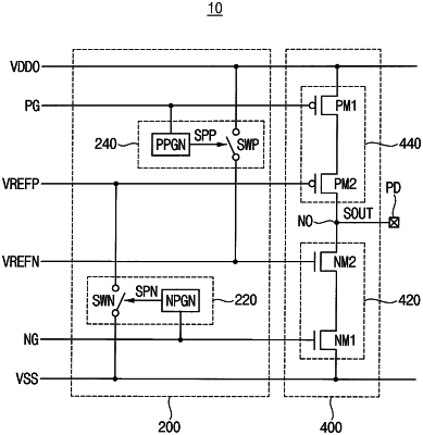
1. An output driver comprising:
a pull-up driver connected between an output power supply voltage and an output node, and configured to pull up a voltage at the output node based on a pull-up driving signal and a pull-up reference voltage, wherein the pull-up reference voltage is generated by a voltage regulator which operates based on the output power supply voltage and a ground voltage;
a pull-down driver connected between the output node and the ground voltage, and configured to pull down the voltage at the output node based on a pull-down driving signal and a pull-down reference voltage, wherein the pull-down reference voltage is generated by the voltage regulator; and
a reference voltage compensation circuit configured to perform a short operation during transitions of the pull-up driving signal and the pull-down driving signal, wherein the short operation comprises electrically connecting any one or any combination of the pull-up reference voltage to the ground voltage, and the pull-down reference voltage to the output power supply voltage.
|