| CPC H03K 19/1776 (2013.01) [G11C 11/412 (2013.01); H03K 19/01721 (2013.01); H03K 19/0944 (2013.01)] | 13 Claims |
|
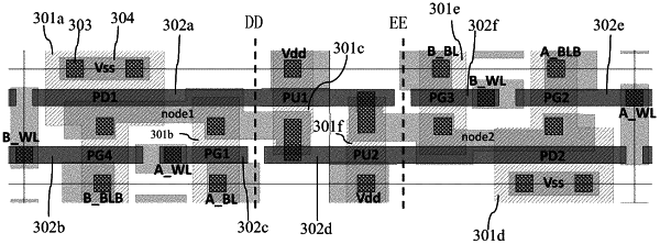
1. A dual-port SRAM cell structure, comprising:
a data memory unit main structure, a first port structure, and a second port structure;
wherein the data memory unit main structure comprises:
a first inverter and a second inverter cross-coupled to each other, and a first memory node and a second memory node mutually inverted to each other;
wherein the first port structure comprises a first pass gate and a second pass gate, and wherein the second port structure comprises a third pass gate and a fourth pass gate;
wherein the first inverter comprises a first pull up transistor and a first pull down transistor;
wherein the second inverter comprises a second pull up transistor and a second pull down transistor;
wherein the first pull up transistor and the second pull up transistor are both PMOS transistors; and
wherein the first pull down transistor, the second pull down transistor, the first pass gate, the second pass gate, the third pass gate, and the fourth pass gate are all NMOS transistors;
wherein the dual-port SRAM cell structure is designed with a cell layout structure, which comprises a first subunit layout structure and a second subunit layout structure that are centrosymmetric to each other;
wherein the first subunit layout structure comprises layouts of the first pull down transistor, the first pull up transistor, the first pass gate, and the fourth pass gate;
wherein the second subunit layout structure comprises layouts of the second pull down transistor, the second pull up transistor, the second pass gate, and the third pass gate;
wherein the first subunit layout structure further comprises:
a first active region, a second active region, and a third active region, wherein the second active region is located between the first active region and the third active region, and wherein the first active region, the second active region, and the third active region are arranged in sequence in a first direction and extend in a second direction perpendicular to the first direction;
wherein the first pull up transistor is arranged in the third active region;
wherein the first pull down transistor is located in the first active region, and a drain region of the first pull down transistor is configured to be the first memory node;
wherein a metal conductive material layer of a metal gate of the first pull up transistor and a metal conductive material layer of a metal gate of the first pull down transistor are electrically connected to form a first metal gate strip extending in the first direction, wherein a P-type metal work function layer in the metal gate of the first pull up transistor and an N-type metal work function layer in the metal gate of the first pull down transistor share a boundary of first work function layers, wherein the boundary is disposed on a top of a field oxide layer between the first active region and the third active region;
wherein the second active region is arranged between the first active region and the third active region;
wherein a first space located between the boundary of first work function layers and the first active region and a second space between the boundary of first work function layers and the third active region are set to meet design rules in the layout structures; wherein a source region of one of the first pass gate and the fourth pass gate is located in the first active region and configured to connect to the first memory node;
wherein a source region of another one of the first pass gate and the fourth pass gate is located in the second active region and is configured to connect to the first memory node via a contact hole and a first metal layer; and
wherein read paths passing through the metal conductive material layers connected to the first memory nodes are centrosymmetric;
wherein the second subunit layout structure comprises:
a fourth active region, a fifth active region, and a sixth active region arranged in sequence in the first direction, wherein the fifth active region is located between the fourth active region and the sixth active region, and wherein the fourth active region, the fifth active region, and the sixth active region extend along the second direction;
wherein the second pull up transistor is disposed in the sixth active region;
wherein the second pull down transistor is disposed in the fourth active region, and wherein a drain region of the second pull down transistor is configured to be the second memory node;
wherein a metal conductive material layer of a metal gate of the second pull up transistor and a metal conductive material layer of a metal gate of the second pull down transistor are connected to form a second metal gate strip extending along the first direction;
wherein a P-type metal work function layer of the metal gate of the second pull up transistor and an N-type metal work function layer formed by the metal gate of the second pull down transistor share a boundary of second work function layers, wherein said boundary is disposed on a top of a field oxide layer between the fourth active region and the sixth active region;
wherein a third space located between the boundary of the second work function layers and the fourth active region, and a fourth space between the boundary of second work function layers and the sixth active region are set to meet design rules in the layout structures; and
wherein a source region of one of the second pass gate and the third pass gate is located in the fourth active region and is configured to connect to the second memory node;
wherein a source region of another one of the second pass gate and the third pass gate is located in the fifth active region and is connected to the second memory node via a contact hole and the first metal layer; and
wherein read paths passing through the metal conductive material layers connected to the second memory node are centrosymmetric;
wherein the fourth pass gate is disposed in the first active region, and the first pass gate is formed in the second active region;
wherein in the first active region, the fourth pass gate and the first pull down transistor are arranged along the second direction; and
wherein a metal conductive material layer of a metal gate of the fourth pass gate and a metal conductive material layer of a metal gate of the first pass gate are aligned with the second metal gate strip.
|