US 12,009,812 B2
Optically switched IGBT
David H. Crowne, Weybridge, VT (US); Richard A. Poisson, Avon, CT (US); and Scott R. Durkee, New Haven, VT (US)
Assigned to Simmonds Precision Products, Inc., Vergennes, VT (US)
Filed by Simmonds Precision Products, Inc., Vergennes, VT (US)
Filed on Sep. 14, 2021, as Appl. No. 17/474,835.
Claims priority of provisional application 63/082,210, filed on Sep. 23, 2020.
Prior Publication US 2022/0094357 A1, Mar. 24, 2022
Int. Cl. H03K 17/785 (2006.01); G02B 6/42 (2006.01); H01L 31/11 (2006.01); H03K 17/16 (2006.01); H04B 10/25 (2013.01)
CPC H03K 17/785 (2013.01) [G02B 6/4295 (2013.01); H01L 31/11 (2013.01); H03K 17/168 (2013.01); H04B 10/25 (2013.01)] 16 Claims
OG exemplary drawing
 
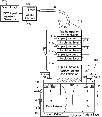
1. A switching device comprising:
an insulated gate bipolar transistor (IGBT) or MOSFET having a gate, an emitter, and a collector configured to allow current to pass between the emitter and the collector based on voltage applied to the gate; and
a stack of alternating layers of photo-sensitive p-n junction layers and insulating layers stacked on the gate for optical switching control of voltage through the IGBT or MOSFET.