US 12,009,795 B2
Method of manufacturing acoustic wave device with multi-layer piezoelectric substrate
Benjamin Paul Abbott, Irvine, CA (US); and Rei Goto, Osaka (JP)
Assigned to Skyworks Solutions, Inc., Irvine, CA (US)
Filed by Skyworks Solutions, Inc., Irvine, CA (US)
Filed on Dec. 11, 2020, as Appl. No. 17/119,904.
Application 17/119,904 is a continuation of application No. 17/067,543, filed on Oct. 9, 2020, abandoned.
Claims priority of provisional application 62/913,614, filed on Oct. 10, 2019.
Claims priority of provisional application 62/913,590, filed on Oct. 10, 2019.
Prior Publication US 2021/0111689 A1, Apr. 15, 2021
Int. Cl. H03H 3/08 (2006.01); H03H 3/04 (2006.01); H10N 30/40 (2023.01); H10N 30/50 (2023.01)
CPC H03H 3/08 (2013.01) [H10N 30/40 (2023.02); H03H 2003/0435 (2013.01); H10N 30/50 (2023.02)] 20 Claims
OG exemplary drawing
 
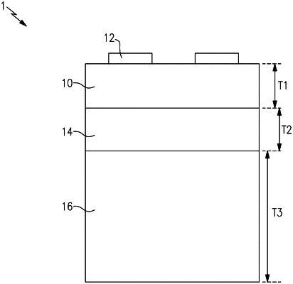
1. A method of manufacturing an acoustic wave device, the method comprising:
bonding a support substrate to a first side of a z-propagation quartz layer with a first Euler angle φ in a range from 40° to 50°, a second Euler angle θ in a range from 85° to 95°, and a third Euler angle ψ in a range of 85° to 95°;
bonding a lithium based piezoelectric layer to a second side of the z-propagation quartz layer, the second side being opposite to the first side; and
forming an interdigital transducer electrode to a side of the lithium based piezoelectric layer that is opposite the z-propagation quartz layer.