| CPC H03B 5/36 (2013.01) [H03B 5/04 (2013.01); H03B 5/32 (2013.01); H03H 9/0547 (2013.01); H03H 9/0552 (2013.01); H03H 9/1021 (2013.01); H03B 2200/0088 (2013.01)] | 9 Claims |
|
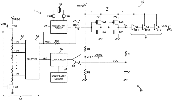
1. A circuit device comprising:
an output circuit including a waveform-shaping circuit configured to waveform-shape an oscillation signal, and configured to output an output clock signal based on a clock signal subjected to the waveform-shaping by the waveform-shaping circuit;
a bias voltage output circuit configured to output a bias voltage of the oscillation signal input to the waveform-shaping circuit;
a comparator configured to compare a DC voltage obtained by smoothing the clock signal subjected to the waveform-shaping with a reference voltage;
a logic circuit configured to set an adjustment value of the bias voltage of the bias voltage output circuit; and
a storage circuit, wherein
in a test mode of the circuit device, the logic circuit changes the adjustment value to determine a set value of the adjustment value based on output of the comparator when the adjustment value is changed, and stores the determined set value in the storage circuit.
|