| CPC H02M 3/1588 (2013.01) [H02M 3/1584 (2013.01); H02M 3/1586 (2021.05)] | 7 Claims |
|
1. A power source device comprising:
an input line that receives a supply of a direct-current input voltage; an output line that is connected to a load;
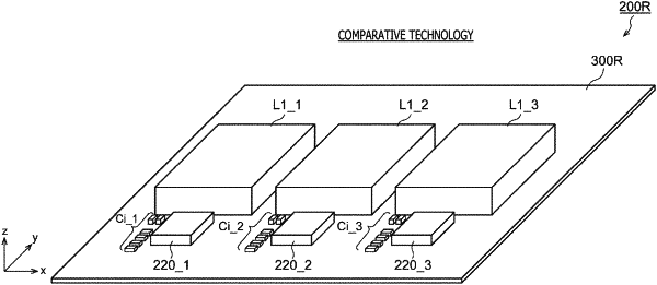
N inductors that correspond to N phases and each have one end connected to the output line, where N is an integer greater than zero and the N inductors are mounted to a main mounting surface of a printed circuit board; and
N power modules that correspond to the N phases and each have an input pin, a switching
pin, and a ground pin, the input pin being connected to the input line, the switching pin being connected to another end of a corresponding inductor, the ground pin being grounded, wherein:
at least one of the N power modules is mounted on a sub-mounting surface that is opposite to the main mounting surface of the printed circuit board,
the N inductors are linearly arranged in a first direction, wherein the first direction is an X-direction of the printed circuit board, and
an i-th (i=1 to N) power module is disposed adjacently in a second direction, wherein the second direction is a Y-direction of the printed circuit board, to a corresponding i-th inductor, the second direction being perpendicular to the first direction.
|