| CPC H02J 7/007194 (2020.01) [G11C 11/401 (2013.01); H01M 10/0525 (2013.01); H01M 10/425 (2013.01); H01M 10/4257 (2013.01); H01M 10/48 (2013.01); H01M 10/486 (2013.01); H01M 10/613 (2015.04); H01M 10/615 (2015.04); H01M 10/625 (2015.04); H01M 10/633 (2015.04); H02J 7/0029 (2013.01); H02J 7/0047 (2013.01); H01L 27/0629 (2013.01); H01M 2010/4271 (2013.01); H01M 2220/20 (2013.01)] | 6 Claims |
|
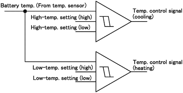
1. A charge control circuit of a secondary battery, comprising:
a temperature sensor for sensing a temperature of the secondary battery;
a first temperature comparison circuit and a second temperature comparison circuit provided with an analog signal from the temperature sensor to generate a pulse signal;
a heating device of the secondary battery which operates in two temperature ranges set by the first temperature comparison circuit;
a cooling device of the secondary battery which operates in two temperature ranges set by the second temperature comparison circuit; and
a memory means which is configured to hold an analog signal,
wherein the memory means comprises a transistor using an oxide semiconductor for a semiconductor layer, a capacitor, a first wiring, a second wiring, and a third wiring,
wherein the transistor comprises a first gate and a second gate,
wherein a first terminal of the transistor is electrically connected to the first wiring,
wherein a second terminal of the transistor is electrically connected to a first terminal of the capacitor,
wherein the first gate of the transistor is electrically connected to the second wiring, and
wherein the second gate of the transistor is electrically connected to the third wiring.
|