| CPC H01S 5/34333 (2013.01) [H01S 5/22 (2013.01)] | 7 Claims |

|
1. A semiconductor light emitting device comprising:
a nitride semiconductor substrate having, as a principal plane, a plane inclined from a c-plane in an m-axis direction in a range from 60° to 90° both inclusive;
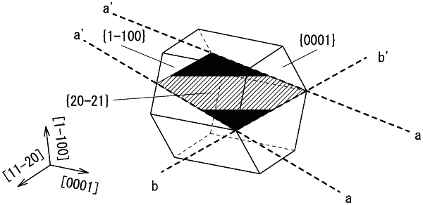
an underlayer provided on the nitride semiconductor substrate and including a first layer and a second layer that are stacked on each other, the first layer including Alx2Inx1Ga(1-x1-x2)N (0<<x1<1, 0≤x2<1) and having a dislocation along an intersection line of the principal plane of the nitride semiconductor substrate and a (1-100) plane, the second layer including Aly2Iny1Ga(1-y1-y2)N (0<y1<1, 0≤y2<1) and having a dislocation along an intersection line of the principal plane of the nitride semiconductor substrate and a (0001) plane; and
a device layer including an active layer provided on the underlayer,
wherein an indium (In) content x1 of the first layer and an indium (In) content y1 of the second layer satisfy Expression (1) below:
0.5%≤y1<6%≤x1≤100% (1).
|