US 12,009,636 B2
Wavelength-variable laser
Junji Yoshida, Tokyo (JP); Hirokazu Itoh, Tokyo (JP); Satoshi Irino, Tokyo (JP); Yuichiro Irie, Tokyo (JP); and Taketsugu Sawamura, Tokyo (JP)
Assigned to FURUKAWA ELECTRIC CO., LTD., Tokyo (JP)
Filed by FURUKAWA ELECTRIC CO., LTD., Tokyo (JP)
Filed on Feb. 3, 2023, as Appl. No. 18/164,285.
Application 18/164,285 is a division of application No. 17/187,086, filed on Feb. 26, 2021, granted, now 11,605,935.
Application 17/187,086 is a continuation of application No. 16/672,163, filed on Nov. 1, 2019, granted, now 10,938,183, issued on Mar. 2, 2021.
Application 16/672,163 is a continuation in part of application No. 16/029,285, filed on Jul. 6, 2018, granted, now 10,511,150, issued on Dec. 17, 2019.
Application 16/029,285 is a continuation in part of application No. 15/454,444, filed on Mar. 9, 2017, granted, now 10,020,638, issued on Jul. 10, 2018.
Application 15/454,444 is a continuation of application No. 14/795,387, filed on Jul. 9, 2015, granted, now 9,601,905, issued on Mar. 21, 2017.
Application 14/795,387 is a continuation of application No. 14/507,374, filed on Oct. 6, 2014, granted, now 9,083,150, issued on Jul. 14, 2015.
Application 14/507,374 is a continuation of application No. PCT/JP2013/060391, filed on Apr. 4, 2013.
Claims priority of provisional application 61/621,013, filed on Apr. 6, 2012.
Prior Publication US 2023/0187906 A1, Jun. 15, 2023
This patent is subject to a terminal disclaimer.
Int. Cl. H01S 5/00 (2006.01); H01S 3/067 (2006.01); H01S 5/02251 (2021.01); H01S 5/02253 (2021.01); H01S 5/10 (2021.01); H01S 5/20 (2006.01); H01S 5/22 (2006.01); H01S 5/227 (2006.01); H01S 5/32 (2006.01); H01S 5/34 (2006.01); H01S 5/343 (2006.01); B82Y 20/00 (2011.01); H01S 3/04 (2006.01); H01S 3/094 (2006.01); H01S 3/0941 (2006.01); H01S 3/30 (2006.01); H01S 5/024 (2006.01); H01S 5/028 (2006.01); H01S 5/14 (2006.01)
CPC H01S 5/3216 (2013.01) [H01S 3/0675 (2013.01); H01S 3/06754 (2013.01); H01S 5/02251 (2021.01); H01S 5/02253 (2021.01); H01S 5/1064 (2013.01); H01S 5/2018 (2013.01); H01S 5/2077 (2013.01); H01S 5/2205 (2013.01); H01S 5/2206 (2013.01); H01S 5/227 (2013.01); H01S 5/3213 (2013.01); H01S 5/34 (2013.01); H01S 5/3406 (2013.01); H01S 5/34306 (2013.01); H01S 5/3434 (2013.01); B82Y 20/00 (2013.01); H01S 3/04 (2013.01); H01S 3/094003 (2013.01); H01S 3/094011 (2013.01); H01S 3/09415 (2013.01); H01S 3/302 (2013.01); H01S 5/0064 (2013.01); H01S 5/024 (2013.01); H01S 5/0287 (2013.01); H01S 5/1039 (2013.01); H01S 5/146 (2013.01); H01S 5/2222 (2013.01); H01S 2301/03 (2013.01); H01S 2301/166 (2013.01)] 11 Claims
OG exemplary drawing
 
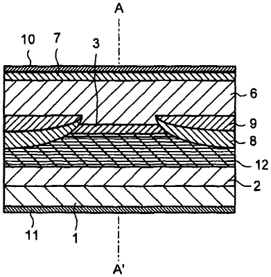
1. An optical semiconductor device outputting a predetermined wavelength of laser light comprising:
a quantum well active layer positioned between a p-type cladding layer and an n-type cladding layer in thickness direction;
a separate confinement heterostructure layer positioned between the quantum well active layer and the n-type cladding layer; and
an electric-field-distribution-control layer positioned between the separate confinement heterostructure layer and the n-type cladding layer and configured by at least two semiconductor layers having band gap energy greater than band gap energy of a barrier layer constituting the quantum well active layer, wherein the optical semiconductor device is fabricated on a GaAs substrate.