| CPC H01Q 9/0421 (2013.01) [H01Q 1/42 (2013.01); H01Q 1/48 (2013.01); H01Q 1/526 (2013.01)] | 10 Claims |
|
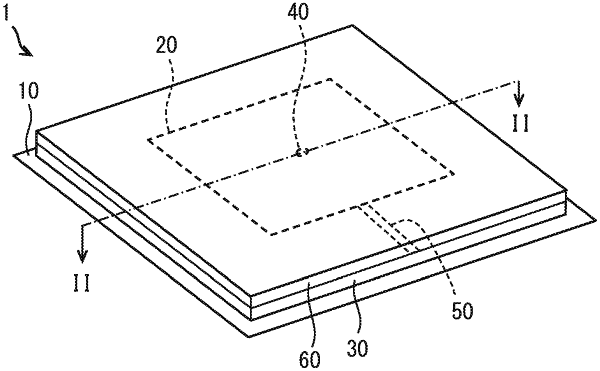
1. An antenna device comprising:
a ground plate made of a conductor with a flat plate shape;
an opposing conductive plate made of another conductor with a flat plate shape, arranged to space apart from the ground plate by a predetermined distance, and having a power supply point electrically connected to a power supply line;
a short-circuit portion electrically connecting the opposing conductive plate and the ground plate; and
a radio wave shield body for shielding a propagation of an electric field, which is arranged on an upper side of the opposing conductive plate and is made of a conductor or a dielectric material, wherein:
parallel resonance at a predetermined target frequency is generated by an inductance provided in the short-circuit portion and a capacitance between the ground plate and the opposing conductive plate; and
the radio wave shield body is arranged so as to contact with an upper surface of an edge portion of the opposing conductive plate.
|