| CPC H01Q 3/267 (2013.01) [H01P 1/2007 (2013.01); H01P 5/19 (2013.01); H04B 7/0617 (2013.01); H04B 7/086 (2013.01)] | 14 Claims |
|
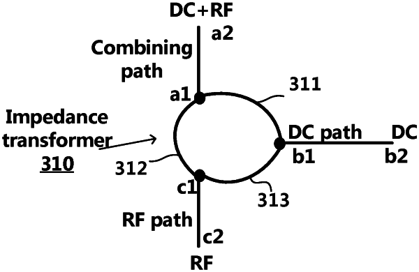
1. A bias tee circuit, comprising:
a combining path having a first end and a second end that is configured to transmit a combined signal which comprises a combination of a radio frequency (RF) signal and a direct current (DC) signal,
an RF path having a first end and a second end that is configured to transmit the RF signal included in the combined signal,
a DC path having a first end and a second end that is configured to transmit the DC signal included in the combined signal, and
an impedance transformer connected between the first end of the combining path, the first end of the RF path, and the first end of the DC path that is configured to make a reflection coefficient of the RF signal transmitted between the second end of the combining path and the second end of the RF path have at least two resonant modes within an operating RF band.
|