| CPC H01Q 1/40 (2013.01) [H01Q 1/243 (2013.01); H01Q 1/38 (2013.01); H01Q 1/52 (2013.01)] | 20 Claims |
|
1. A terminal device, comprising:
a housing comprising an outer surface;
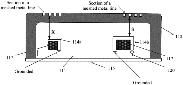
a metal line that is either disposed on the outer surface or is embedded in the housing, wherein the metal line is configured to receive or send an electromagnetic wave signal, wherein the metal line is a translucent metal line and comprises a metal mesh, wherein the metal mesh is coated with a metal layer, wherein the metal layer is configured to reduce impedance of the metal mesh, wherein a transmittance of the metal line is Y, and wherein a value range of Y is 50%≤Y≤95%;
a circuit board configured to hold electronic parts and components; and
a signal line disposed on the circuit board and forming a gap between the signal line and the metal line,
wherein the signal line and the metal line are configured to feed the electromagnetic wave signal through the gap in a coupling manner.
|