| CPC H01Q 1/243 (2013.01) [H01Q 1/48 (2013.01); H01Q 5/25 (2015.01); H01Q 5/307 (2015.01); H01Q 9/0407 (2013.01)] | 20 Claims |
|
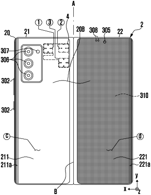
1. An electronic device comprising:
a housing providing a front surface of the electronic device and a rear surface of the electronic device;
an antenna structure including a printed circuit board located within the housing and including a first surface facing the front surface or the rear surface and a second surface facing an opposite direction to the first surface, wherein the printed circuit board comprises:
a first conductive layer including a first antenna element and a second antenna element that do not overlap each other when viewed from above the first surface;
a second conductive layer located closer to the second surface than the first conductive layer and operating as a ground plane; and
a dielectric located between the first conductive layer and the second conductive layer; and
a conductive pattern that overlaps at least a part of the second conductive layer when viewed from above the first surface;
wherein, when the first surface faces the rear surface, the conductive pattern is located between the front surface and the second surface; and
wherein, when the first surface faces the front surface, the conductive pattern is located between the rear surface and the second surface.
|