| CPC H01Q 1/2283 (2013.01) [H01L 23/3107 (2013.01); H01L 23/552 (2013.01); H01L 23/66 (2013.01); H01L 24/13 (2013.01); H01Q 1/22 (2013.01); H01Q 1/52 (2013.01); H01Q 1/526 (2013.01); H01Q 19/30 (2013.01); H01Q 21/0087 (2013.01); H01Q 21/24 (2013.01); H01L 23/3128 (2013.01); H01L 2223/6616 (2013.01); H01L 2223/6677 (2013.01); H01L 2224/02331 (2013.01); H01L 2224/02379 (2013.01); H01L 2224/0401 (2013.01); H01L 2224/05024 (2013.01); H01L 2224/13023 (2013.01); H01L 2224/13024 (2013.01); H01L 2224/18 (2013.01); H01L 2924/19102 (2013.01); H01L 2924/3025 (2013.01); H01Q 15/14 (2013.01); H01Q 21/28 (2013.01)] | 20 Claims |
|
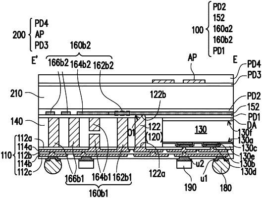
1. A package structure, comprising:
a first redistribution circuit structure;
a semiconductor die, disposed over and electrically coupled to the first redistribution circuit structure;
a first insulating encapsulation, encapsulating the semiconductor die;
a first antenna and a second antenna, electrically coupled to the semiconductor die, wherein in a vertical projection, the first antenna and the second antenna are offset from the semiconductor die, and wherein a propagating direction of an electromagnetic wave generated from the first antenna is different from a propagating direction of an electromagnetic wave generated from the second antenna; and
a first metallic layer, disposed over the first insulating encapsulation, wherein in the vertical projection, the first metallic layer is overlapped with the semiconductor die, and wherein the first metallic layer comprises:
first signal patterns, electrically coupled to the semiconductor die; and
a first antenna ground, electrically isolated from the semiconductor die.
|