| CPC H01Q 1/2283 (2013.01) [H01Q 1/243 (2013.01); H01Q 1/52 (2013.01); H01Q 3/2635 (2013.01); H01Q 3/40 (2013.01); H01Q 5/42 (2015.01); H01Q 5/48 (2015.01); H01Q 11/14 (2013.01); H01Q 21/062 (2013.01); H01Q 21/245 (2013.01); H01Q 21/28 (2013.01)] | 28 Claims |

|
1. A portable communication device, comprising:
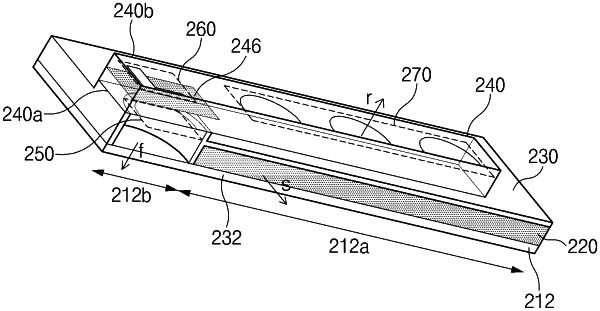
a housing including a conductive member and a glass layer, the glass layer forming a portion of an outer surface of the portable communication device, the housing including at least one opening formed in a portion of the conductive member;
a first antenna array accommodated in the housing and facing in a first direction, the first antenna array including at least one antenna element facing the at least one opening; and
a second antenna array accommodated in the housing and facing in a second direction,
wherein the at least one opening is located between the glass layer and the first antenna array,
wherein a non-conductive member is disposed on the at least one antenna element and between the glass layer and the first antenna array, and
wherein an opaque layer is located at least between the non-conductive member and the glass layer.
|