| CPC H01L 33/62 (2013.01) [G02F 1/13452 (2013.01); H01L 23/5387 (2013.01); H01L 25/0753 (2013.01); H01L 33/005 (2013.01); H01L 2933/0066 (2013.01)] | 20 Claims |
|
1. A display device, comprising:
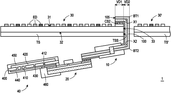
a pixel array substrate, having a first surface, a second surface opposite to the first surface, and a first side surface connecting the first surface and the second surface, wherein a plurality of bonding pads are located on the first surface; and
a circuit board, electrically connected to the bonding pads, bent from above the first surface of the pixel array substrate to below the second surface, wherein the circuit board comprises a thermoplastic substrate, wherein the thermoplastic substrate comprises a third surface facing the pixel array substrate and a fourth surface opposite to the third surface, and the thermoplastic substrate comprises a first bend formed by thermoplastics.
|