| CPC H01L 33/44 (2013.01) [H01L 33/005 (2013.01); H01L 33/56 (2013.01); H01L 33/58 (2013.01); H01L 2933/0025 (2013.01); H01L 2933/0091 (2013.01)] | 12 Claims |
|
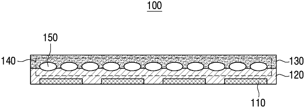
1. A display panel comprising:
a light emitting device;
a first protection layer which is disposed on an upper portion of the light emitting device, and of which surface is treated for diffuse reflection;
a second protection layer which is disposed on an upper portion of the first protection layer, and of which surface is treated for at least one of diffuse reflection and anti-reflection; and
a transparent layer which includes transparent materials that transmit visible rays, and absorb or reflect ultraviolet rays and infrared rays,
wherein the transparent materials are spaced apart from each other with a predetermined interval and fixed on the surface of the first protection layer between the first protection layer and the second protection layer.
|