| CPC H01L 33/22 (2013.01) [H01L 33/0093 (2020.05); H01L 33/0095 (2013.01); H01L 33/32 (2013.01)] | 12 Claims |
|
1. A manufacturing method of a light-emitting diode structure, the method comprising:
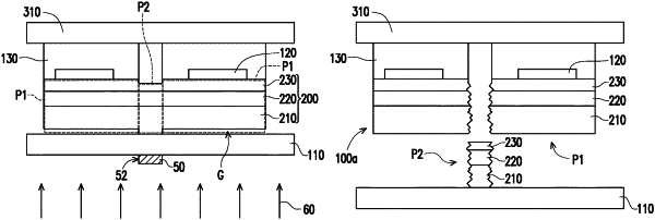
growing a semiconductor stack layer on a first substrate, wherein the semiconductor stack layer is divided into a first portion and a second portion, and comprises a first type semiconductor layer, an active layer, and a second type semiconductor layer sequentially grown on the first substrate;
providing a force applying means to physically break the first portion and the second portion apart from each other, wherein the first portion comprises a plurality of light-emitting diode structures separated from each other; and
before providing the force applying means to break the first portion and the second portion apart from each other, irradiating, by a laser, a boundary between the first portion and the first substrate or a boundary between the second portion and the first substrate to reduce a binding force between the first portion and the first substrate or reduce a binding force between the second portion and the first substrate.
|