US 12,009,449 B2
Solar cell having an emitter region with wide bandgap semiconductor material
Richard M. Swanson, Los Altos, CA (US); Marius M. Bunea, Santa Clara, CA (US); Michael C. Johnson, Alameda, CA (US); David D. Smith, Campbell, CA (US); Yu-Chen Shen, Sunnyvale, CA (US); Peter J. Cousins, Los Altos, CA (US); and Tim Dennis, Canton, TX (US)
Assigned to Maxeon Solar Pte. Ltd., Singapore (SG)
Filed by Maxeon Solar Pte. Ltd., Singapore (SG)
Filed on Feb. 9, 2023, as Appl. No. 18/107,917.
Application 18/107,917 is a division of application No. 17/183,164, filed on Feb. 23, 2021, granted, now 11,605,750.
Application 17/183,164 is a continuation of application No. 16/692,890, filed on Nov. 22, 2019, granted, now 10,957,809, issued on Mar. 23, 2021.
Application 16/692,890 is a continuation of application No. 16/230,968, filed on Dec. 21, 2018, granted, now 10,490,685, issued on Nov. 26, 2019.
Application 16/230,968 is a continuation of application No. 14/945,708, filed on Nov. 19, 2015, granted, now 10,170,657, issued on Jan. 1, 2019.
Application 14/945,708 is a continuation of application No. 14/706,773, filed on May 7, 2015, granted, now 9,219,173, issued on Dec. 22, 2015.
Application 14/706,773 is a continuation of application No. 13/429,138, filed on Mar. 23, 2012, granted, now 9,054,255, issued on Jun. 9, 2015.
Prior Publication US 2023/0197877 A1, Jun. 22, 2023
Int. Cl. H01L 21/00 (2006.01); H01L 31/0216 (2014.01); H01L 31/0224 (2006.01); H01L 31/0236 (2006.01); H01L 31/068 (2012.01); H01L 31/072 (2012.01); H01L 31/0745 (2012.01); H01L 31/0747 (2012.01); H01L 31/18 (2006.01)
CPC H01L 31/0747 (2013.01) [H01L 31/02167 (2013.01); H01L 31/022441 (2013.01); H01L 31/02363 (2013.01); H01L 31/068 (2013.01); H01L 31/0682 (2013.01); H01L 31/072 (2013.01); H01L 31/0745 (2013.01); H01L 31/18 (2013.01); H01L 31/1804 (2013.01); Y02E 10/547 (2013.01); Y02P 70/50 (2015.11)] 22 Claims
OG exemplary drawing
 
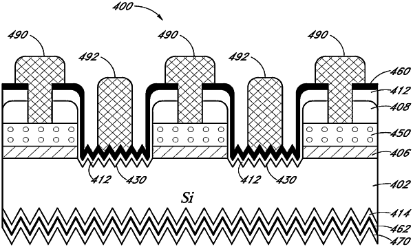
1. A solar cell, comprising:
a semiconductor substrate;
a first thin dielectric layer disposed on the semiconductor substrate;
a first semiconductor region of a first conductivity type disposed on the first thin dielectric layer;
a second thin dielectric layer disposed on the semiconductor substrate; and
a second semiconductor region of a second conductivity type disposed on the second thin dielectric layer, the second conductivity type opposite the first conductivity type, wherein the second thin dielectric layer is disposed on a sidewall surface of the first semiconductor region, and the second dielectric layer laterally separates the first and second semiconductor regions.