| CPC H01L 31/048 (2013.01) [H01L 31/0543 (2014.12); H01L 31/068 (2013.01); H01L 31/1824 (2013.01); H01L 31/1868 (2013.01)] | 16 Claims |
|
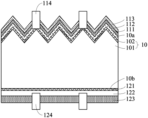
1. A solar cell, comprising:
a substrate having a front surface and a rear surface opposite to the front surface;
a first passivation layer, a second passivation layer and a third passivation layer sequentially formed on the front surface and in a direction away from the front surface; wherein the first passivation layer includes a dielectric material; the second passivation layer includes a first silicon nitride SimNn material, and a ratio of n/m is 0.5˜1; the third passivation layer includes a silicon oxynitride SiOiNj material, and a ratio of j/i is 0.1˜0.6; and
a tunneling oxide layer and a doped conductive layer sequentially formed on the rear surface and in a direction away from the rear surface, wherein the doped conductive layer and the substrate have doping elements of a same conductivity type;
wherein the dielectric material is an aluminum oxide AlxOy material, and a ratio of y/x is 1.1˜1.5; and
wherein the ratios y/x, n/m and j/i are atomic ratios;
wherein the solar cell further comprises a fourth passivation layer formed on a side of the doped conductive layer facing away from the substrate, the fourth passivation layer includes a second silicon nitride SiaNb material, and a ratio of a/b is 3.5˜6.8; and
wherein the fourth passivation layer includes a plurality of sub-layers, and refractive indices of the plurality of sub-layers gradually decrease in a direction from the rear surface toward the doped conductive layer.
|