| CPC H01L 31/02167 (2013.01) [H01L 31/02363 (2013.01); H01L 31/035281 (2013.01)] | 30 Claims |
|
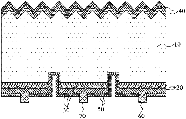
1. A cell assembly, comprising:
a silicon substrate;
a first doped region and a second doped region, alternately disposed on a back side of the silicon substrate and having opposite polarities;
a first dielectric layer, disposed on a front side of the silicon substrate;
a second dielectric layer, wherein an orthogonal projection of at least a portion of the second dielectric layer onto the silicon substrate is disposed between orthogonal projections of the first doped region and the second doped region along a lateral direction of the silicon substrate; and
a first conductive layer and a second conductive layer, respectively disposed in the first doped region and the second doped region;
wherein:
the first doped region comprises a first doped layer, a passivation layer, and a second doped layer;
the first doped layer of the first doped region is a part of the silicon substrate;
the passivation layer of the first doped region is provided on the first doped layer of the first doped region; and
the second doped layer of the first doped region is provided on the passivation layer of the first doped region, and is connected to the first doped layer of the first doped region through the passivation layer of the first doped region.
|