| CPC H01L 29/7869 (2013.01) [H01L 21/02565 (2013.01); H01L 21/47635 (2013.01); H01L 21/477 (2013.01); H01L 27/1225 (2013.01); H01L 27/1251 (2013.01); H01L 27/1259 (2013.01); H01L 29/24 (2013.01); H01L 29/41733 (2013.01); H01L 29/42356 (2013.01); H01L 29/42384 (2013.01); H01L 29/45 (2013.01); H01L 29/66969 (2013.01); H01L 29/78621 (2013.01); H01L 29/78645 (2013.01); H01L 29/78648 (2013.01)] | 2 Claims |
|
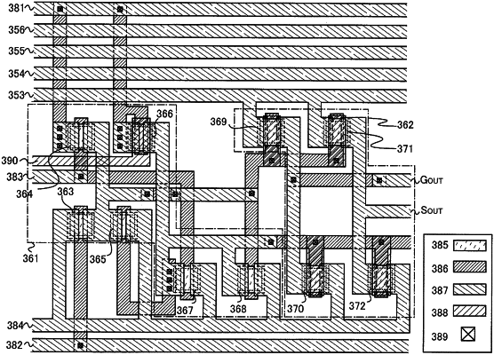
1. A semiconductor device comprising:
a first transistor, a second transistor, a third transistor, a fourth transistor, and a fifth transistor,
wherein one of a source and a drain of the first transistor is electrically connected to one of a source and a drain of the fifth transistor and a first wiring,
wherein the first wiring has a function of transmitting a signal which is output from a circuit comprising the first transistor, the second transistor, the third transistor, the fourth transistor, and the fifth transistor,
wherein a first conductive layer has a function of a gate of the first transistor,
wherein a second conductive layer has a function of one of a source and a drain of the third transistor and one of a source and a drain of the fourth transistor,
wherein a third conductive layer has a function of a gate of the second transistor,
wherein the first conductive layer is electrically connected to the third conductive layer through the second conductive layer,
wherein one of a source and a drain of the second transistor is electrically connected to a gate of the third transistor,
wherein the other of the source and the drain of the second transistor is electrically connected to a second wiring,
wherein the other of the source and the drain of the third transistor is electrically connected to the second wiring,
wherein the gate of the third transistor is electrically connected to a gate of the fifth transistor, and
wherein the second transistor comprises a channel formation region over and overlapping with the third conductive layer.
|