| CPC H01L 29/78678 (2013.01) [H01L 21/28194 (2013.01); H01L 29/0649 (2013.01); H01L 29/41733 (2013.01); H01L 29/42384 (2013.01); H01L 29/66765 (2013.01); H01L 29/7869 (2013.01)] | 8 Claims |
|
1. A thin film transistor, comprising:
a substrate;
a gate electrode over the substrate;
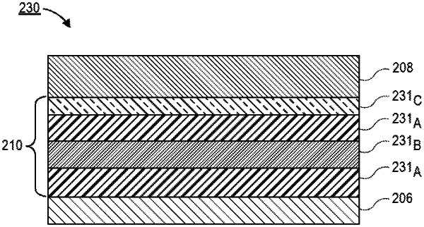
a gate dielectric stack over the gate electrode, wherein the gate dielectric stack comprises a plurality of layers, the plurality of layers comprising a first layer of 1, 2, 11, 12, 14, 18, 20, and 22, a layer of Al2O3 on the first layer of HfO2, and a second layer of HfO2 on the layer of Al2O3, wherein a first one of the plurality of layers has a first thickness, and a second one of the plurality of layers has a second thickness different than the first thickness;
a semiconductor layer over the gate dielectric stack, wherein the semiconductor layer comprises a crystalline semiconductor layer in direct contact with the second layer of HfO2 of the gate dielectric stack; and
a source electrode and a drain electrode, both the source electrode and the drain electrode directly on and in contact with the crystalline semiconductor layer, wherein the gate electrode extends laterally at least as wide as the semiconductor layer and at least as wide as the gate dielectric stack.
|