| CPC H01L 29/7851 (2013.01) [H01L 21/02252 (2013.01); H01L 21/3065 (2013.01); H01L 21/32139 (2013.01); H01L 29/66795 (2013.01)] | 10 Claims |
|
1. A method of patterning a gate structure on a substrate, the method comprising:
providing a patterned mask layer on the substrate, the patterned mask layer corresponding to a gate pattern;
providing an upper gate layer underlying the patterned mask layer, the upper gate layer comprising silicon;
providing a bottom gate layer underlying the upper gate layer, the bottom gate layer comprising silicon germanium (Si1-xGex), wherein a ratio of silicon to germanium in the Si1-xGex is 0.1<X<0.4;
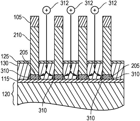
plasma etching the upper gate layer and the bottom gate layer with a halogen-based plasma to form the gate pattern in the upper gate layer and the bottom gate layer and form the gate structure, wherein the halogen-based plasma etches the bottom gate layer faster than the upper gate layer to reduce formation of silicon germanium residues near a bottom of the gate structure; and
after plasma etching the upper gate layer and the bottom gate layer, oxidizing the upper gate layer and the bottom gate layer to: (a) oxidize sidewall surfaces of the gate structure to form a sidewall oxide on the sidewall surfaces of the gate structure, and (b) oxidize any silicon germanium residues formed during the plasma etching to form oxide compounds near the bottom of the gate structure, the oxide compounds comprising a silicon germanium oxide (Si1-xGexOz) complex;
wherein said oxidizing preferentially oxidizes the silicon germanium residues formed near the bottom of the gate structure as opposed to oxidizing the sidewall surfaces of the gate structure.
|