| CPC H01L 29/785 (2013.01) [H01L 21/823443 (2013.01); H01L 21/823821 (2013.01); H01L 29/41791 (2013.01); H01L 29/4975 (2013.01); H01L 29/66795 (2013.01)] | 20 Claims |
|
1. A device comprising:
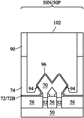
a gate structure over a channel region of a substrate;
a source/drain region adjacent the channel region;
a first inter-layer dielectric over the source/drain region;
a silicide between the first inter-layer dielectric and the source/drain region, the silicide contacting a top surface of the source/drain region and a bottom surface of the source/drain region;
a first void exposing a surface of the silicide and the bottom surface of the source/drain region; and
a first source/drain contact having a first portion and a second portion, the first portion of the first source/drain contact disposed between the silicide and the first inter-layer dielectric, the second portion of the first source/drain contact extending through the first inter-layer dielectric and contacting the silicide.
|