| CPC H01L 29/7827 (2013.01) [H01L 29/41775 (2013.01); H01L 29/66666 (2013.01)] | 20 Claims |
|
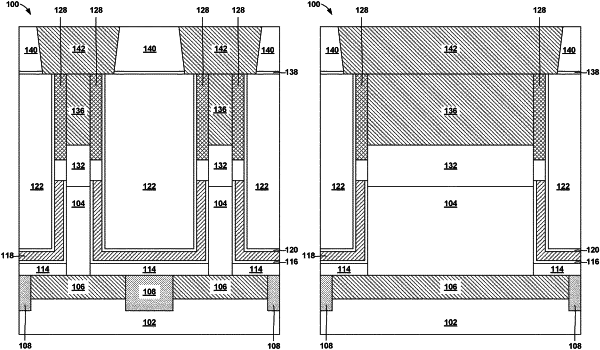
1. A semiconductor structure comprising:
a bottom source drain region arranged on a substrate;
a semiconductor channel region extending vertically upwards from a top surface of the bottom source drain region;
a metal gate disposed around the semiconductor channel region;
a top source drain region above the semiconductor channel region; and
a top contact partially embedded into the top source drain region
a dielectric spacer separating the metal gate from the top source drain region, wherein a width of the dielectric spacer is substantially equal to a width of the top source drain region.
|