| CPC H01L 29/66969 (2013.01) [H01L 29/24 (2013.01); H01L 29/78696 (2013.01)] | 20 Claims |
|
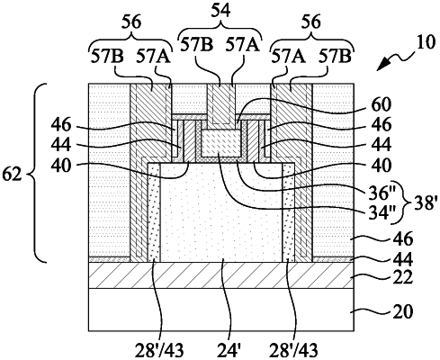
1. A method of manufacturing a semiconductor device, the method comprising:
forming a dielectric fin over a dielectric layer;
forming a ring encircling and contacting sidewalls of the dielectric fin, the ring comprising a two-dimensional semiconductor material, wherein the forming the ring comprises:
conformally depositing the two-dimensional semiconductor material; and
removing portions of the two-dimensional semiconductor material to form the ring;
forming a gate dielectric contacting top surfaces of the dielectric fin, the dielectric layer, and the two-dimensional semiconductor material;
forming a gate electrode over the gate dielectric; and
forming a source/drain contact plug contacting the two-dimensional semiconductor material.
|