US 12,009,410 B2
Semiconductor device and method fabricating the same
Zhi-Chang Lin, Hsinchu County (TW); Wei-Hao Wu, Hsinchu (TW); and Jia-Ni Yu, New Taipei (TW)
Assigned to TAIWAN SEMICONDUCTOR MANUFACTURING CO., LTD., Hsinchu (TW)
Filed by TAIWAN SEMICONDUCTOR MANUFACTURING CO., LTD., Hsinchu (TW)
Filed on Apr. 17, 2023, as Appl. No. 18/301,712.
Application 17/339,795 is a division of application No. 16/142,672, filed on Sep. 26, 2018, granted, now 11,031,489, issued on Jun. 8, 2021.
Application 18/301,712 is a continuation of application No. 17/339,795, filed on Jun. 4, 2021, granted, now 11,631,754.
Prior Publication US 2023/0253482 A1, Aug. 10, 2023
Int. Cl. H01L 29/66 (2006.01); H01L 23/535 (2006.01); H01L 29/06 (2006.01); H01L 29/08 (2006.01); H01L 29/78 (2006.01)
CPC H01L 29/6681 (2013.01) [H01L 23/535 (2013.01); H01L 29/0649 (2013.01); H01L 29/0847 (2013.01); H01L 29/7851 (2013.01)] 20 Claims
OG exemplary drawing
 
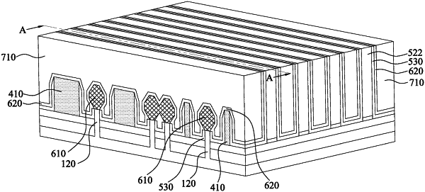
1. A semiconductor device, comprising:
a substrate;
a semiconductor fin extending along a first direction on the substrate;
a dielectric fin disposed on the substrate and extending substantially parallel to the semiconductor fin;
a gate structure across the semiconductor fin and the dielectric fin; and
gate spacers disposed on opposite sidewalls of the gate structure, wherein an interface between the gate structure and the dielectric fin is lower than an interface between the dielectric fin and one of the gate spacers.